Appearance
Behavior
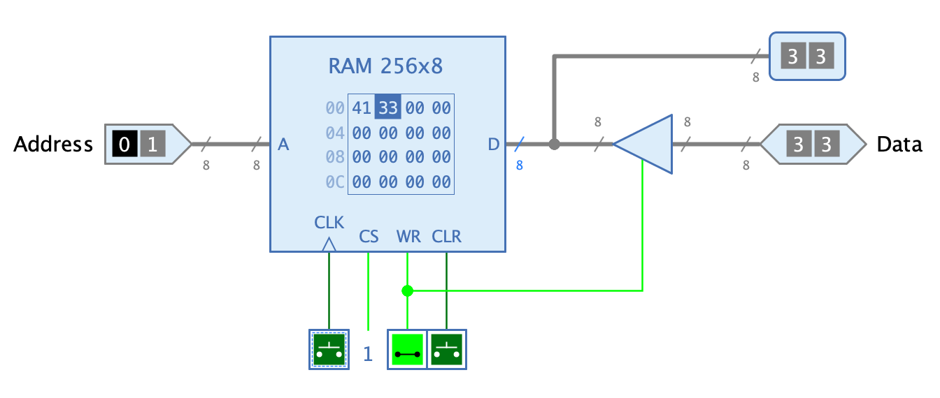
The RAM is a memory component whose data can be read and written by the using circuit during simulation.
The contents of the memory cells of the RAM component can be read and written synchronously via a bidirectional data pin.
The RAM component provides two different interfaces that can be selected via the value of the property "Clock Input".
- Synchronous
-
With this interface the RAM contains the clock input "CLK". If the input "WR" has the value 1, the data present at input "D" is read on the rising edge of the clock input.
- Asynchronous
-
With this interface the RAM does not contain a clock input. If input "WR" has the value 1, the data present at input "D" are read each time they change.
Pins
- A
-
Input "Address": Determines the address of the memory cell whose data is to be read or written.
- CS
-
Input "Chip Select": The RAM component only reads or writes data if this input has the value 1.
- D
-
Input/Output "Data": Outputs the data to be read or accepts the data to be written, depending on the value of inputs "WR" and "CLK". If property "Separate data pins" is selected, this pin acts as output only.
- DI
-
Input Data: Only available if property "Separate data pins" is selected. Accepts the data to be written into the RAM.
- CLK
-
Input "Clock": Is only displayed if the property "Clock Input" is set. At the rising edge of the CLK signal, data is read or written, depending on the value of "WR".
- WR
-
Input "Write": With the value 1 data can be written into the RAM.
- CLR
-
Input "Clear": Asynchronous input at which a value of 1 causes all memory cells to be reset to the value 0, independent of the other inputs.
Properties
See the chapter Memory for a description of the general memory properties. In this section only the special properties of the RAM component are described.
- Separate data pins
-
If set, the RAM has two separate pins for data input "DI" and data output "D". If not set, both data input and data output are handled through the bidirectional pin "D". This property is only enabled if the RAM is not yet connected to wires.
- Clock Input
-
If this property is set, the RAM contains the "CLK" pin. This property is only enabled if the RAM is not yet connected to wires.
- Non-volatile
-
If set, the RAM content is preserved across multiple simulation runs. When the simulation is stopped, Antares stores the currentRAM data in the directory "nonVolatile" in the workspace where the circuit is located. Each RAM instance in different circuits has its own storage location. When restarting the simulation, the data is loaded again into the RAM. Note that since the data isn’t stored in the circuit file, the user doesn’t have to perform "Save".